Dual Layer High Frequency PCB Made On Rogers 20mil RT/duroid 5870
Laminate
Rogers RT/duroid 5870 high frequency material is glass microfiber
reinforced PTFE composites which is designed for exacting stripline
and microstrip circuit applications. The exceptional dielectric
constant uniformity results from its randomly oriented microfibers.
The dielectric constant of RT/duroid 5870 is uniform from panel to
panel and is constant over a wide frequency range. Its low
dissipation factor extends the usefulness of RT/duroid 5870 to
Ku-band and above. RT/duroid 5870 materials are easily cut, sheared
and machined to shape. They are resistant to all solvents and
reagents, hot or cold, normally used in etching printed circuits or
in plating edges and holes.
General description
This is a type of double sided RF PCB built on RT/duroid 5870 for
the application of RF Transceiver.
Basic specifications
Base material: RT/duroid 5870 20mil (0.508mm)
Dielectric constant: 2.20+/-0.02
Layer count: 2 layers
Type: Through holes
Format: 100mm x 150mm = 1 type = 1 piece
Surface finish: Immersion gold
Copper weight: Outer layer 35 μm
Solder mask / Legend: No
Final PCB height: 0.52 mm
Standard: IPC 6012 Class 2
Packing: 20 panels are packed for shipment.
Lead time: 7 working days
Shelf life: 6 months
Features and benefits
Low moisture absorption
Isotropic
Uniform electrical properties over frequency
30000 square meter month capability;
8000 types of PCB's per month;
Quick CADCAM checking and free PCB quotation;
More than 16 years of PCB experience;
Applications
Millimeter Wave Applications, Power splitter, Microstrip Antenna,
Automatic Gate Induction, Missile Guidance Systems
PCB Capability 2021
| Parameter | Value |
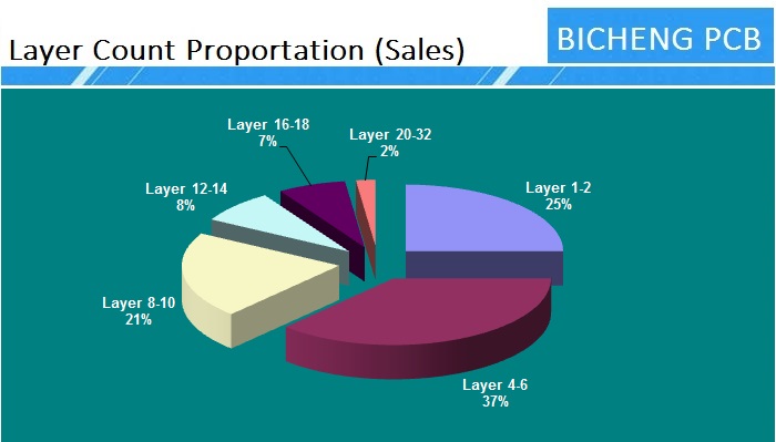
| Layer Counts | 1-32 |
| Substrate Material | FR-4(including High Tg 170, High CTI>600V); Aluminum based;
Copper based; Rogers RO4350B, RO4003C, RO3003, RO3006, RO3010,
RO3210 etc.; Rogers RT/duroid 5880, RT/duroid 5870, RT/duroid 6002,
RT/duroid 6010 etc..; Taconic TLX-8, TLY-5, RF-35TC, TLF-35 etc..;
Arlon AD450, AD600 etc; PTFE F4B DK2.2, DK2.65 etc..; Polyimide and
PET. |
| Maximum Size | Flying test: 900*600mm, Fixture test 460*380mm, No test 1100*600mm |
| Board Outline Tolerance | ±0.0059" (0.15mm) |
| PCB Thickness | 0.0157" - 0.3937" (0.40mm--10.00mm) |
| Thickness Tolerance(T≥0.8mm) | ±8% |
| Thickness Tolerance(t<0.8mm) | ±10% |
| Insulation Layer Thickness | 0.00295" - 0.1969" (0.075mm--5.00mm) |
| Minimum Track | 0.003" (0.075mm) |
| Minimum Space | 0.003" (0.075mm) |
| Outer Copper Thickness | 35µm--420µm (1oz-12oz) |
| Inner Copper Thickness | 17µm--350µm (0.5oz - 10oz) |
| Drill Hole(Mechanical) | 0.0059" - 0.25" (0.15mm--6.35mm) |
| Finished Hole(Mechanical) | 0.0039"-0.248" (0.10mm--6.30mm) |
| DiameterTolerance(Mechanical) | 0.00295" (0.075mm) |
| Registration (Mechanical) | 0.00197" (0.05mm) |
| Aspect Ratio | 12:1 |
| Solder Mask Type | LPI |
| Min Soldermask Bridge | 0.00315" (0.08mm) |
| Min Soldermask Clearance | 0.00197" (0.05mm) |
| Plug via Diameter | 0.0098" - 0.0236" (0.25mm--0.60mm) |
| Impedance Control Tolerance | ±10% |
| Surface Finish | HASL,HASL LF,ENIG,Imm Tin,Imm Ag, OSP, Gold Finger |